
Media


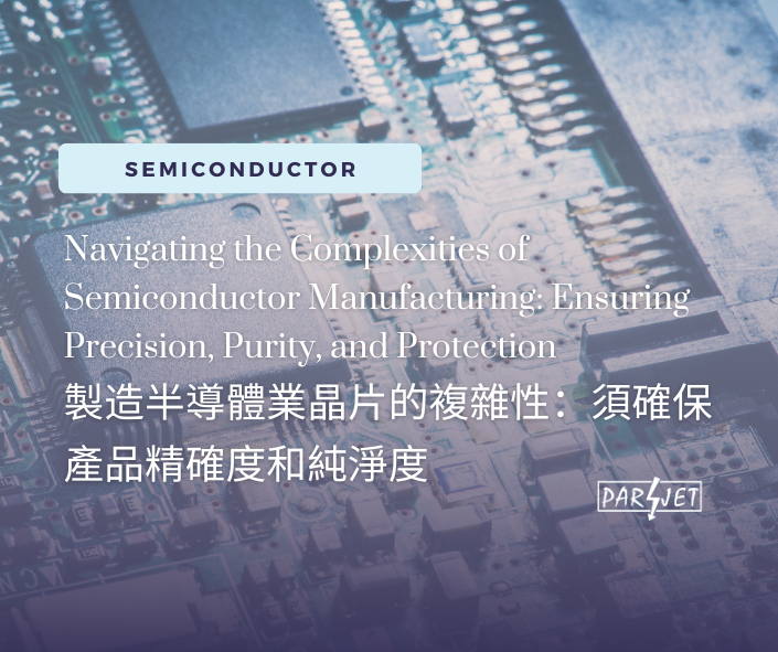
Navigating the Complexities of Semiconductor Manufacturing: Ensuring Precision, Purity, and Protection
Introduction
The semiconductor industry is pivotal in powering modern digital technology, driving advancements from consumer electronics to sophisticated automotive systems. This industry demands not only high precision and ultra-clean manufacturing environments but also effective strategies for managing electromagnetic interference (EMI). This article delves into the critical considerations in semiconductor production and showcases how Parjet’s specialized products, including EMI shielding solutions, support these needs.
High Purity Requirements
In semiconductor manufacturing, the purity of the environment and materials is paramount. Contaminants as small as a single particle can compromise the functionality of semiconductor devices. To combat this, manufacturers implement stringent contamination control measures, utilizing cleanrooms and advanced filtration systems, and adhering to strict protocols to maintain an ultra-pure production environment.
Precision in Fabrication
The intricate process of fabricating semiconductor wafers involves detailed techniques like photolithography and etching, demanding extreme precision. Each step is carefully controlled to ensure the accuracy and functionality of semiconductor circuits, necessitating reliable and precise equipment.
Thermal and Chemical Management
Dealing with high temperatures and corrosive chemicals is standard in semiconductor production. Materials used must withstand these conditions to maintain process stability and ensure product integrity, emphasizing the need for robust material solutions.
Incorporating EMI Shielding
As semiconductor devices become smaller and more complex, managing electromagnetic interference (EMI) becomes crucial. EMI can disrupt the delicate electronic pathways in semiconductors, leading to data loss or device failure. Parjet’s innovative EMI shielding solutions, including helical springs and canted coil springs, are specifically designed to protect sensitive components from electromagnetic disruptions. For an in-depth look at our EMI shielding technologies, read our detailed article: EMI Shielding: Helical (Spiral) Spring and Canted Coil Springs Solutions.
Advanced Material Solutions from Parjet
Parjet’s commitment to the semiconductor industry extends beyond traditional components. Our PTFE seals and EMI shielding solutions are designed to meet the sector's rigorous requirements:
High chemical resistance: Ensures durability against harsh processing chemicals.
Exceptional thermal stability: Maintains performance across various temperature extremes.
Superior purity and EMI protection: Minimizes contamination risks and shields against electromagnetic interference, critical for maintaining the integrity and functionality of semiconductor devices.
Conclusion
The semiconductor industry is a cornerstone of technological innovation, requiring materials and solutions that support its complex demands. Parjet is dedicated to providing the semiconductor industry with advanced materials like PTFE seals and specialized EMI shielding components, ensuring reliability, purity, and precision in semiconductor manufacturing.
Explore Our Solutions
For more information on how Parjet’s products can enhance your semiconductor processes and protect against EMI, visit our semiconductor industry applications page: Parjet Semiconductor Industry Applications.