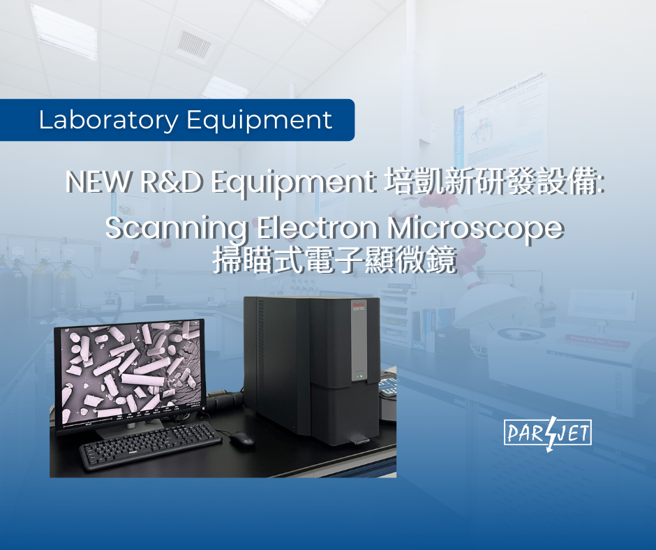
We are happy to share the arrival of our new R&D equipment - Scanning Electron Microscope (SEM).
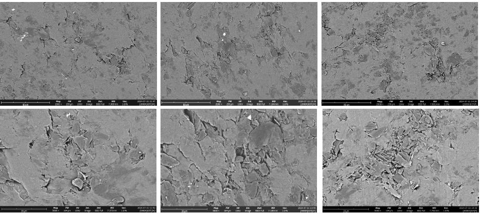
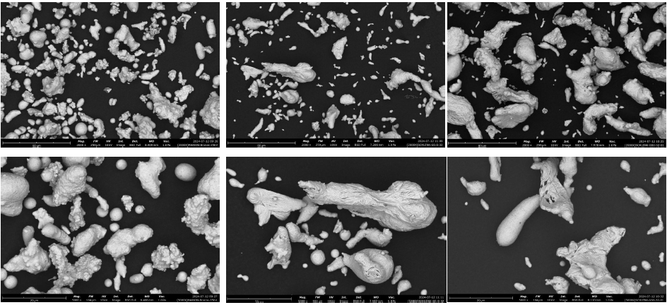
SEM allows us to observe the microstructure of any compounds. It is an important tool to ensures the quality of our products by analyzing the PTFE tubes at different stages. Through the understanding of the physical properties of the semi-finished products, we can further improve our manufacturing techniques and secure the best quality for our clients. SEM can also contribute to finding the reasons behind sealing failures by analyzing the composition of the used seals and identify the potential failure factors.
Testing Abilities:
• Filament: CeB6 long life filament
• Vacuum mode: high/low
• Optical magnification: 20-134X
• Electronic magnification: 160-350,000X
• Resolution: SED ≤ 6nm and BSD ≤ 8nm
• Acceleration voltage: 5kV, 10kV, 15kV (default)
• Sample size: 25mm diameter/35mm height


For more information, please contact us here.


